Ultra-Wideband Digital Conversion and 16-Channel Polyphase Channelization on AMD Versal™ Architecture
This whitepaper details the design and implementation of a high-performance ultra-wideband (UWB) signal processing chain on the AMD Versal™ ACAP. By integrating a 64-GSPS Jariet transceiver with a custom 16-channel Polyphase Channelizer running on AI Engines (AIE), the solution overcomes traditional FPGA logic bottlenecks.
This whitepaper details the design and implementation of a high-performance ultra-wideband (UWB) signal processing chain on the AMD Versal™ ACAP. By integrating a 64-GSPS Jariet transceiver with a custom 16-channel Polyphase Channelizer running on AI Engines (AIE), the solution overcomes traditional FPGA logic bottlenecks.
Introduction
The demand for wider instantaneous bandwidth in next-generation radar, Electronic Warfare (EW), and spectral monitoring systems presents significant processing challenges.
Traditional FPGA architectures struggle to close timing at the clock rates required to process multi-gigahertz streams directly. This project demonstrates a breakthrough architecture leveraging the AMD Versal™ Adaptive Compute Acceleration Platform (ACAP).
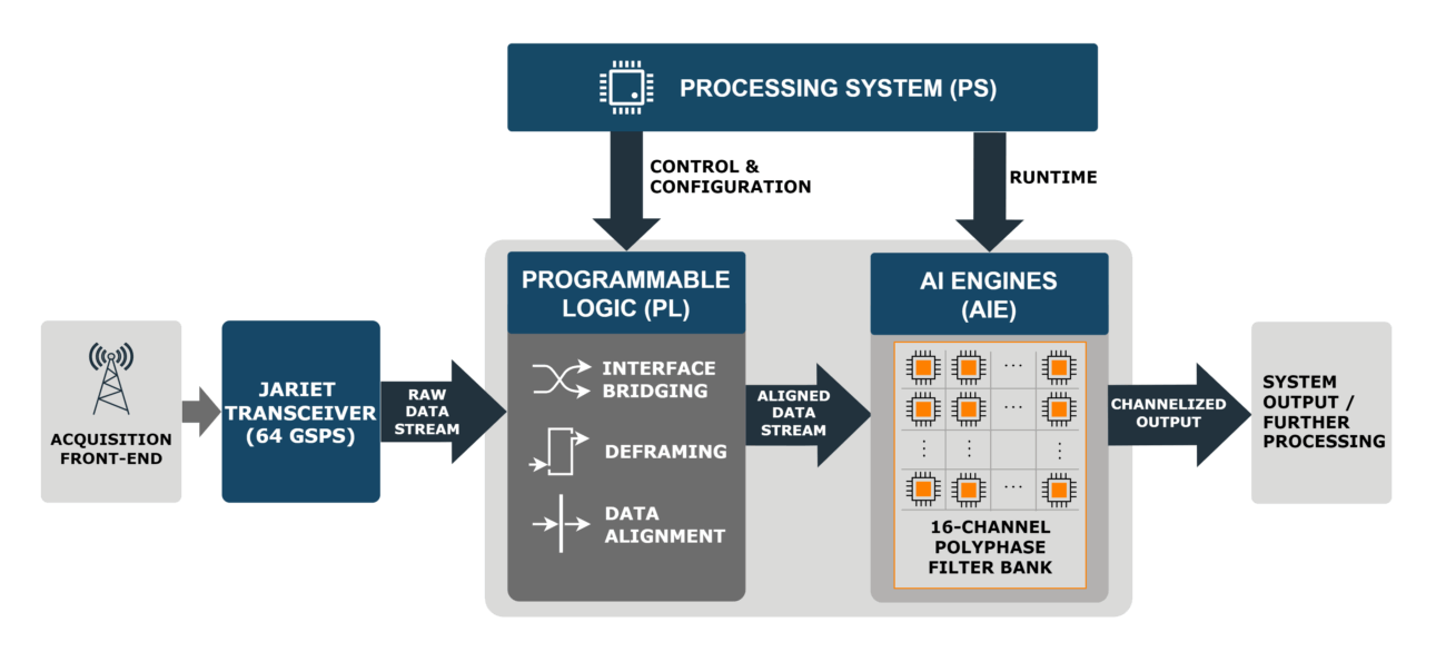
We present a cohesive system that captures a 64 GSPS stream via Jariet wideband converters and efficiently channelizes the spectrum using the Versal AI Engines, moving the compute-intensive filtering burden away from Programmable Logic (PL).
System Architecture Overview
The system is designed as a heterogeneous compute pipeline, partitioned to exploit the specific strengths of each Versal domain:
- Acquisition Front-End: Jariet transceiver operating at 64 GSPS.
- Programmable Logic (PL): Handles high-speed interface bridging, deframing and data alignment.
- AI Engines (AIE): Executes the computationally dense 16-channel Polyphase Filter Bank.
- Processing System (PS): Manages the control plane, configuration, and runtime orchestration.
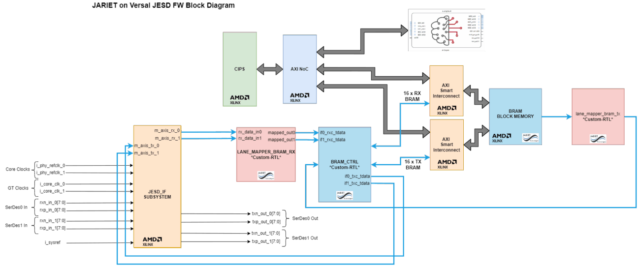
High-Throughput Firmware (FW) Design
Ingesting data at 64 GSPS requires a highly parallelized firmware architecture. The FW design focuses on:
- SerDes & Alignment: Managing the physical lane alignment and synchronization across the Jariet interface.
- Datapath Widening: Converting the serial high-speed stream into a parallel, wide-bus format manageable by the PL clock domains (running at lower frequencies relative to the sampling rate).
- AXI-Stream Formatting: Preparing data packets for transmission over the Network-on-Chip (NoC), ensuring maximum throughput efficiency and zero-packet-loss integrity.
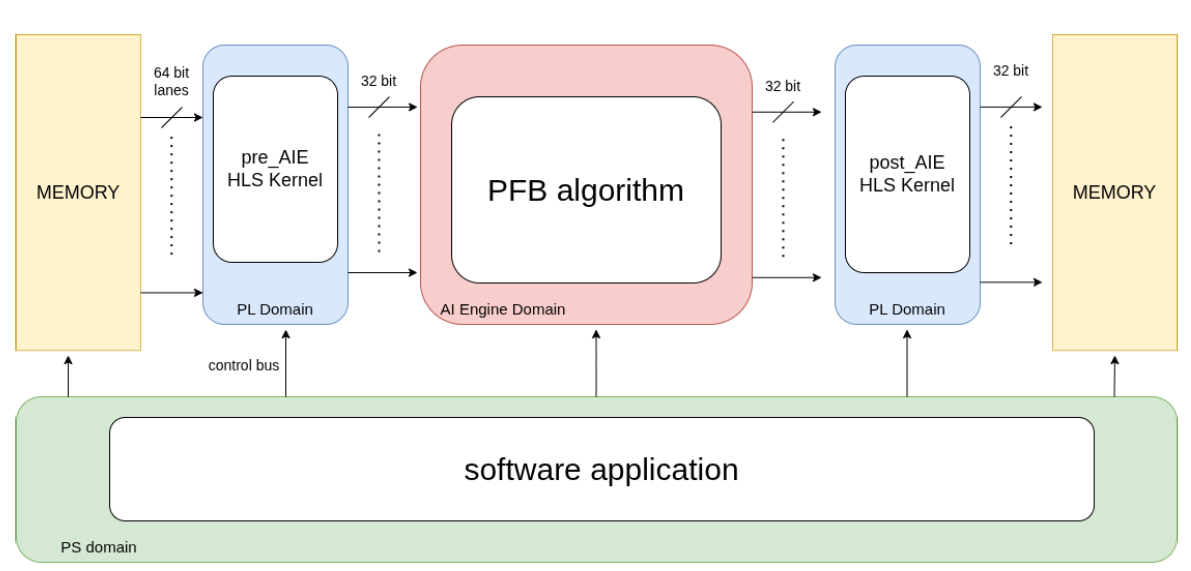
The AIE-Based Polyphase Channelizer
The core innovation of this design is the implementation of a generic N=16 Polyphase Channelizer within the AI Engine array. Unlike traditional DSP48-based implementations, the AIE approach utilizes vector-processor tiles to perform massive parallel filtering operations.
Key implementation details include:
- Vectorization: Utilizing 512-bit vector registers to process multiple samples per clock cycle.
- Memory Tiling: Optimized use of local memory tiles for filter coefficient storage and delay line management.
- Graph-Based Design: The channelizer is defined using the Vitis™ AIE graph model, wallowing the compiler to optimize placement and routing for deterministic latency.
Software & Integration Methodology
To ensure flexibility and ease of operation, the control plane is implemented through a hierarchical three-tier software architecture. This split-design approach decouples the high-level RF configuration from the low-level hardware management.
- Host-Side Runtime Configuration The top layer consists of a Host application responsible for the managing and configuration of the RF Front-End. This software layer manages the high-level parameters of the Jariet transceivers, providing a user-friendly interface for runtime configuration (e.g., gain control, calibration modes, and frequency tuning) without requiring direct interaction with the embedded hardware registers.
- Embedded Communication Bridge (ARM Cortex-A72) Running on the Versal Processing System (PS), this embedded layer acts as the critical bridge between the external Host and the hardware. It manages the communication protocol with the Host, receiving command packets and translating them into low-level Memory-Mapped I/O (MMIO) read/write transactions. This ensures efficient and secure access to the PL and RF subsystems.
- AIE Core PS Application A dedicated embedded application is responsible for the lifecycle management of the AI Engines. Leveraging the Adaptive Data Flow (ADF) APIs, this application loads the graph binary, initializes the AIE array, and manages the graph execution runtime. It ensures the channelizer graph remains synchronized with the data flow coming from the PL.
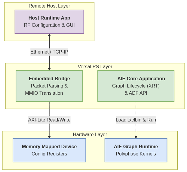
Integration Methodology
The entire stack was developed and integrated using the AMD Vitis™ Unified Software Platform. This methodology allowed for a seamless co-design flow, enabling the simultaneous development of the PS applications, PL kernels, and AIE graphs within a single environment, ensuring correct alignment of memory maps and stream interfaces across all domains.
Conclusion
This implementation validates the capability of D&P Electronic Systems to handle extreme bandwidths (64 GSPS) by offloading DSP tasks to AI Engines on AMD Versal™ devices. The resulting 16-channel polyphase channelizer offers a scalable, power-efficient, and low-latency solution for future wideband RF applications.