FMC JARIET – Ultra-Low Power 64 GSPS Dual Channel Mixed Signal Front End
The FMC JARIET is a high-performance FMC module compliant with the VITA 57.1 specification in a Long-Form (LF) factor. It is specifically designed for applications requiring ultra-low power consumption without compromising on extreme sampling speeds.
This module features a single Jariet Technologies Electra MX device, providing a Dual 10-bit ADC and Dual 10-bit DAC both operating at 64 GSPS. With an analog input and usable bandwidth of 32 GHz, it enables direct RF sampling and synthesis for wideband signals. The interface to the host carrier is managed via 16 lanes of JESD204B/C, reaching speeds up to 30 Gbps for maximum performance.
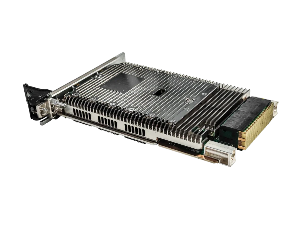
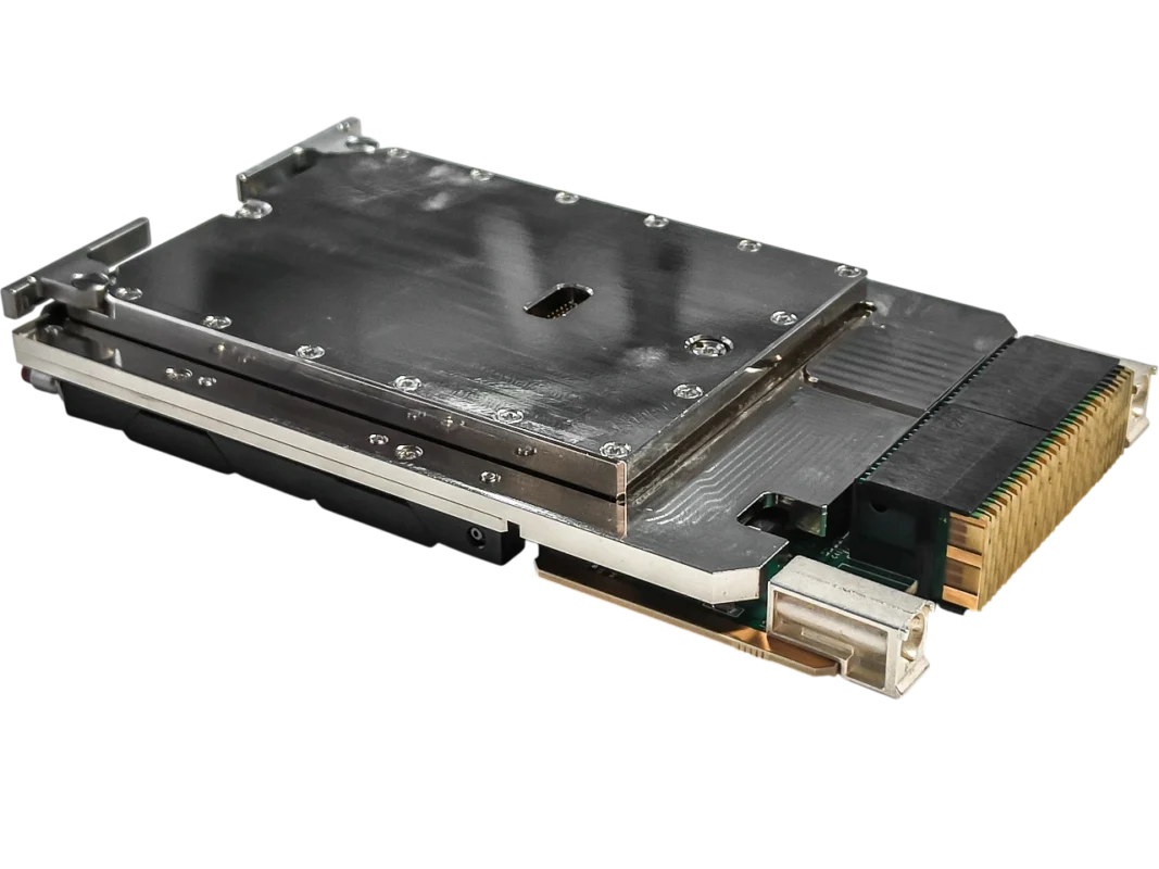
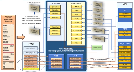
VRS-3UVPX – High-Performance 3U VPX Versal™ FPGA Processor
The VRS-3UVPX is a ruggedized 3U VPX module engineered for real-time, low-latency embedded processing in the most demanding environments. It serves as a high-performance adaptive acceleration platform, integrating the AMD Versal™ Adaptive SoC (XCVC1502) to implement high-throughput signal and data processing pipelines.
This module features advanced backplane connectivity, including PCIe Gen4 x8 and multi-rate Ethernet up to 100GbE, supporting highly scalable VPX architectures. Designed for versatility, it is an ideal engine for applications such as Digital Beamforming, Edge AI/ML inference, and Network Acceleration.
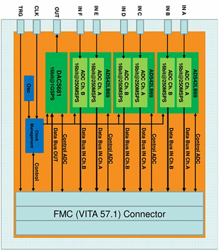
FMC16bit6ADC&1DAC
•3 x Dual ADCs ADS42LB69 by T.I.:
– Resolution: 16 bits;
– Clock up to 250 MHz;
– Instantaneous Bandwidth: 900 MHz;
– Power Dissipation: 1.8 W;
– SNR: 73 dBc@170 MHz (typ)
– SFDR: 87 dBFS@170 MHz (typ).
•DAC DAC5681 by TI:
– Resolution: 16 bits;
– Sample rate up to 1 GSPS;
– Instantaneous Bandwidth: 900 MHz;
– Power Dissipation: 1.0 W @ 1 GSPS, 600 mW @ 500 MSPS, full
operating conditions;
– Single carrier W-CDMA ACLR = 80 dBc @ 80 MHz IF;
– High performance, low noise PLL clock multiplier
– Digital inverse sinc filter.
•Clock Section:
– External Reference up to 350 MHz
– Clock Reference;
– 50 MHz LO (TXCO);
– Distribution of the PLL+VCO output
•Input Trigger signal;
• VITA 57.1 – 2010 compliant (HPC
Connector);
• Conduction Cooled format;
• Conformal Coating (opz);
• Antisulfur resistors (opz);
• Operating Temperature Range: (-40,
+85)°C;
• Operating Humidity Range: 5% to
95% at 40°C non-condensing.
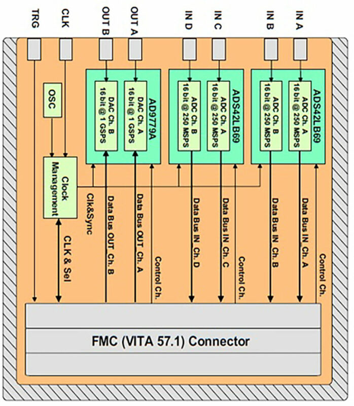
FMC16bit4ADC&2DAC
• 2 x Dual ADCs ADS42LB69 by T.I.:
– Resolution: 16 bits;
– Clock up to 250 MHz;
– Instantaneous Bandwidth: 900 MHz;
– Power Dissipation: 1.8 W;
– SNR: 73 dBc@170 MHz (typ)
– SFDR: 87 dBFS@170 MHz (typ).
• Dual DAC AD9779A by Analog:
– Resolution: 16 bits;
– Sample rate up to 1 GSPS;
– Instantaneous Bandwidth: 900 MHz;
– Power Dissipation: 1.0 W @ 1 GSPS, 600 mW @ 500 MSPS, full
operating conditions;
– Single carrier W-CDMA ACLR = 80 dBc @ 80 MHz IF;
– Novel 2×, 4×, and 8× interpolator/coarse complex modulator;
– High performance, low noise PLL clock multiplier;
Digital inverse sinc filter;
• Clock Section:
– External Reference up to 350 MHz
– Clock Reference;
– 50 MHz LO (TXCO);
– Distribution of the PLL+VCO output
The front connectors are MMCX type
• Input Trigger signal;
• VITA 57.1 – 2010 compliant (HPC Connector);
• Conduction Cooled format;
• Conformal Coating (opz);
• Antisulfur resistors (opz);
• Operating Temperature Range: (-40,
+85)°C;
• Operating Humidity Range: 5% to 95% at 40°C non-condensing.
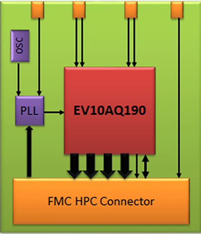
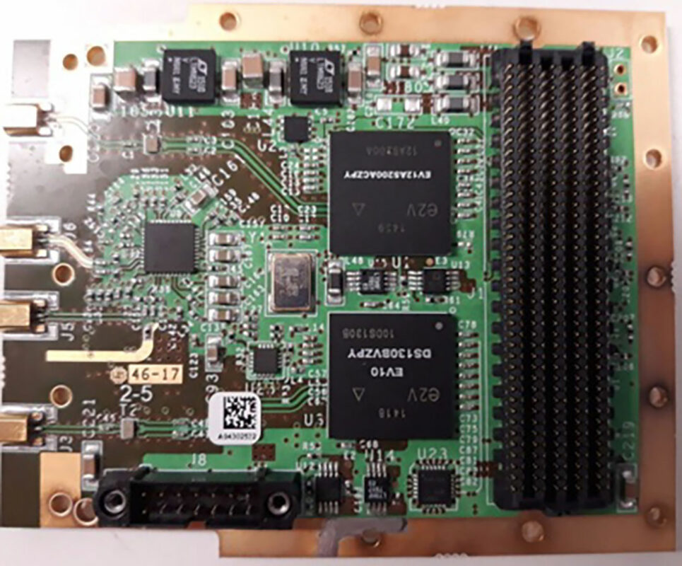
FMC High Speed 10 bit Quad ADC
– Resolution: 10 bits;
– Clock up to 5000 MHz (1-channel conf);
– Four Channels (1, 2 or 4 input configuration):
1. Two Single ended inputs;
2. Two Differiantial inputs (matched).
– Internal clock generation;
– Instantaneous Bandwidth
1. Single ended inputs 40 to 3000 MHz;
2. Two Differiantial inputs up to 3 GHz.
– Power Dissipation: 3 W.
•Internal PLL:
– Internal TCXO;
– External reference (alternative to TCXO);
•External SYNC
•Input SYNC signal;
• VITA 57.1 – 2010 compliant (HPC Connector);
• Conduction Cooled format;
• Conduction Cooled format;
• Conformal Coating (opz);
• Antisulfur resistors (opz);
• Operating Temperature Range: (-40,
+85)°C;
• Operating Humidity Range: 5% to
95% at 40°C non-condensing.
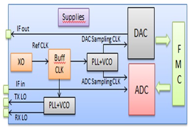
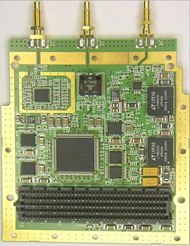
FMC High Speed Dual ADC and DAC
– Resolution: 12 bits;
– Clock up to 1500 MHz;
– Singe ended Input;
– Internal clock generation;
– Instantaneous Bandwidth: 400-3000 MHz;
– Power Dissipation: 3 W.
•DAC EV10DS130 by E2V:
– Resolution: 10 bits;
– Clock up to 3000 MHz;
– Singe ended Output;
– Internal clock generation;
– Instantaneous Bandwidth: 400-3000 MHz;
– Power Dissipation: 1.6 W (MUX 1:2).
•Two internal PLL (Internal TCXO):
– PLL for internal clock generation (ADC, DAC);
– PLL for external clock generation (OUT1, PUT2).
•Input SYNC signal;
• VITA 57.1 – 2010 compliant (HPC Connector);
• Conduction Cooled format;
• Conduction Cooled format;
• Conformal Coating (opz);
• Antisulfur resistors (opz);
• Operating Temperature Range: (-40,
+85)°C;
• Operating Humidity Range: 5% to
95% at 40°C non-condensing.
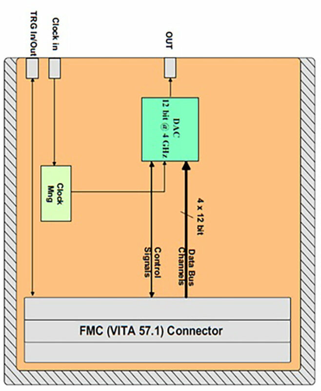
FMC HS SYNTHESIZER
• RF Output Characteristics:
− Single ended (A.C. coupled);
− Up to 3rd Nyquist Band Usable Analog Outputs (Clk = 4 GHz).
•Clk Input Characteristics:
− Single ended clock;
− Direct or PLL Distribution mode;
− PLL Input frequency mode: (0.5 – 350) MHz.
•DAC Characteristics (MD653D by Euvis):
− DAC Resolution 12-bit;
− 1:4 Demultiplexed Digital LVDS Inputs;
− Sampling Clock = 4 GHz;
− True Single Core Architecture;
− Output Voltage Span: 800 mVpp
• 4 W Power Consumption;
• Input Trigger signal;
• FMC format (VITA57.1) Conduction Cooled;
• Operative temperature Range: (-40 , +85)°C;
• Conformal Coating opz.
• FMC IP Cores available (VHDL language)• Input SYNC signal;
• Input SYNC signal;
• Conduction Cooled format;
• Conformal Coating (opz);
• Antisulfur resistors (opz);
•Operating Temperature Range: (-40, +85)°C;
• Operating Humidity Range: 5% to 95% at 40°C non-condensing.
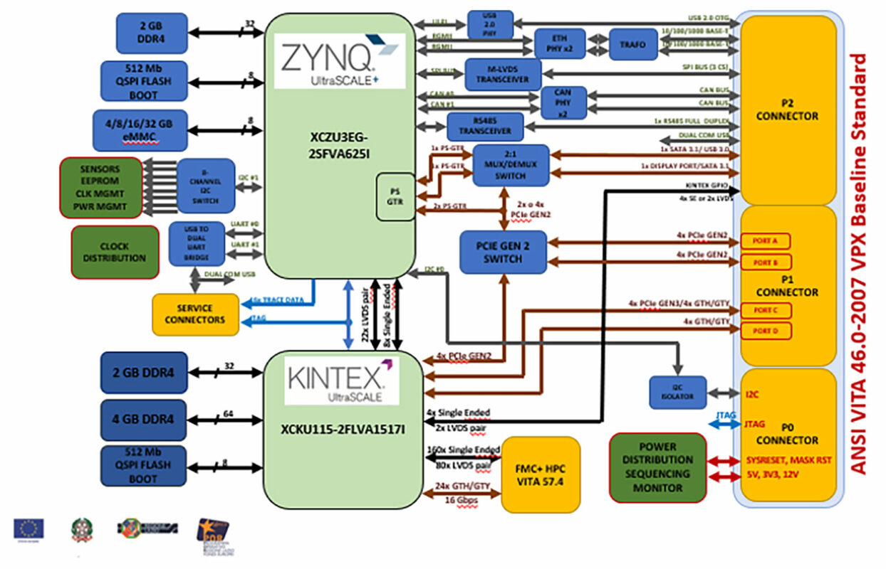
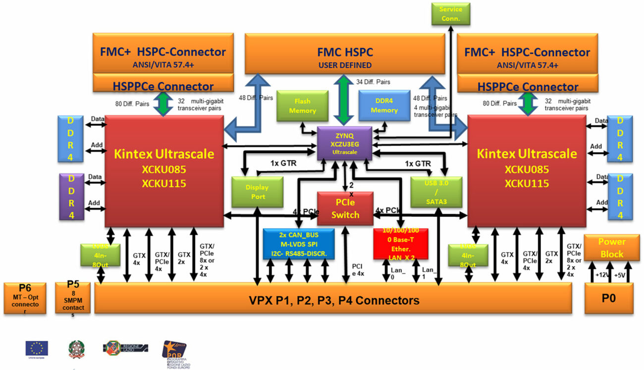
Kintex&ZynqUS_3UVPX_ Board
• ZYNQ: XCZU3EG-2SFVA625I
• ZYNQ external Memory
− DDR4: 2 GB (x32) DDR4 -1600
− Flash Memory : 64 MB
− eMMC: 4/8/16/32 GB
•Processor Peripherals :
− GPIO, 2 x CAN BUS, 2 x I2C, 1 x SPI BUS
• ZYNQ external Memory
− 16 flexible & configurable ports (x1, x4 or x8)
− Four DMA Channels
− Dual Cast
•FPGA: Kintex Ultrascale XCKU115, XCKU095, XCKU085 FLVA1517,
•FPGA external memory:
− DDR4 memory : 1 bank 4 GB (x64) + 1 bank 2 GB (x32) DDR4 -1600
− Flash memory : 64 MB (x8)
− Sampling Clock = 4 GHz;
• Connectors: According to VITA 46.0/VITA 65.0 (P0,P1,P2), and to VITA 57.4 (P3)
• P0 : Power & System signals
• P1 : Two x4 fabric ports mapped as per VITA 46.0, that can be configured as:
− Port A, B : One x4 PCIe Gen2 Port, connected to PCIe Switch
− Port C : One x4 fabric Port (4 lanes connected to FPGA PCIe GEN3 or GTH/GTY)
• P2 : 1x USB 2.0, 2x Gigabit Ethernet, 1x SATA 3.1, 1x DISPLAY PORT, 2x CAN BUS, 1x USB (2x debug UART), 1x SPI
• P3 : FMC high-pin count connector according to VITA 57.4, extended support from 10 to 24 GT + 80 differential pairs
• VPX 3U Air or Conduction cooled Mechanical frame.
Kintex&ZynqUS_6UVPX_ Board
• ZYNQ: XCZU3EG-2SFVA625I
• ZYNQ external Memory
− DDR4: 2 GB (x32) DDR4 -1600
− Flash Memory : 64 MB
− eMMC: 4/8/16/32 GB
•Processor Peripherals :
− GPIO, 2 x CAN BUS, 2 x I2C, 1 x SPI BUS
• ZYNQ external Memory
− 16 flexible & configurable ports (x1, x4 or x8)
− Four DMA Channels
− Dual Cast
•FPGA: Kintex Ultrascale XCKU115, XCKU095, XCKU085 FLVA1517,
•FPGA external memory:
− DDR4 memory : 1 bank 4 GB (x64) + 1 bank 2 GB (x32) DDR4 -1600
− Flash memory : 64 MB (x8)
− Sampling Clock = 4 GHz;
• Connectors: According to VITA 46.0/VITA 65.0 (P0,P1,P2), and to VITA 57.4 (P3)
• P0 : Power & System signals
• P1 : Two x4 fabric ports mapped as per VITA 46.0, that can be configured as:
− Port A, B : One x4 PCIe Gen2 Port, connected to PCIe Switch
− Port C : One x4 fabric Port (4 lanes connected to FPGA PCIe GEN3 or GTH/GTY)
• P2 : 1x USB 2.0, 2x Gigabit Ethernet, 1x SATA 3.1, 1x DISPLAY PORT, 2x CAN BUS, 1x USB (2x debug UART), 1x SPI
• P3 : FMC high-pin count connector according to VITA 57.4, extended support from 10 to 24 GT + 80 differential pairs
• VPX 3U Air or Conduction cooled Mechanical frame.
Analog Receiver in Ku band
•Operative bandwidth:(14.1 - 15.7) GHz
•Sensitivity: -150 dBw (-120dBm)
•Maximum input signal: -100 dBw (-70 dBm)
•Noise Figure <9 dB
•Gain chain: 80 dB
•Operative temperature: 25°
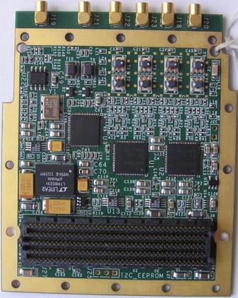
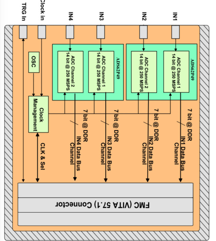
FMC Quad 14 bit ADC
•Two Dual ADCs ADS62P49 by T.I.:
•Resolution: 14 bits;
•Clock up to 250 MHz;
•Input Bandwidth selection (opz.); Instantaneous Bandwidth: 500 MHz; Power Dissipation: 1.25 W; •SFDR: 95 dBc @170 MHz (typ) SINAD: 70 dBFS@170 MHz (typ).
•External or internal Clock Generation;
•Input Trigger signal;
FMC IP Cores available (VHDL language). The front connectors are MMCX type.
•VITA 57.1 – 2010 compliant (HPC Connector);
•Conduction Cooled;
•Conformal Coating (opz);
•Anti-Sulfur Resistor type
•Operating Temperature Range: (-40, +85) °C;
•Operating Humidity Range:
5% to 95% at 40°C non-condensing