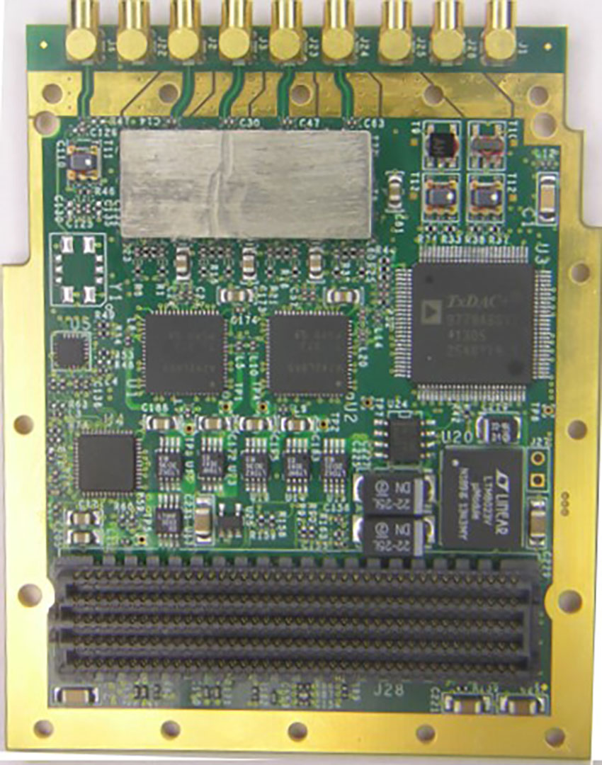
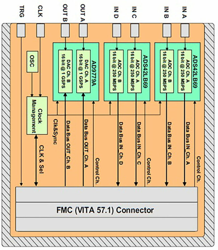
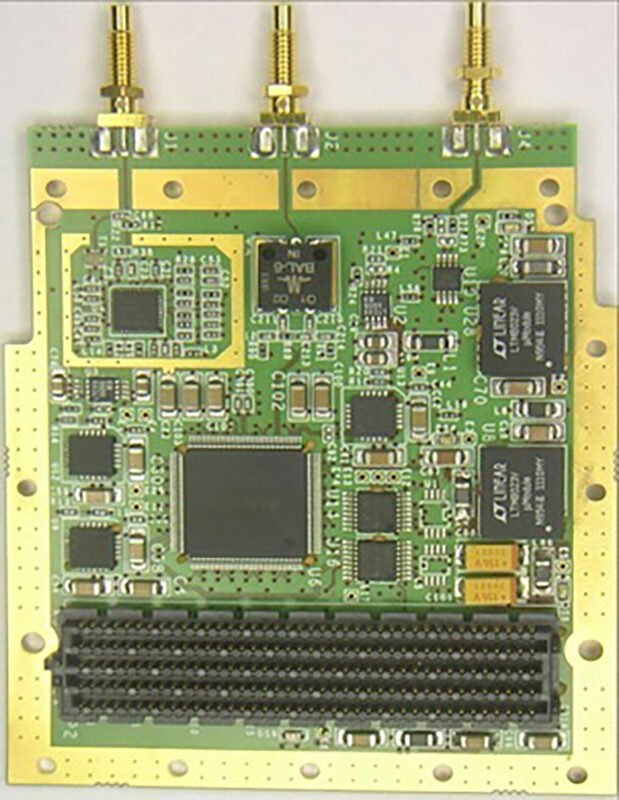
FMC16bit4ADC&2DAC
• 2 x Dual ADCs ADS42LB69 by T.I.:
– Resolution: 16 bits;
– Clock up to 250 MHz;
– Instantaneous Bandwidth: 900 MHz;
– Power Dissipation: 1.8 W;
– SNR: 73 dBc@170 MHz (typ)
– SFDR: 87 dBFS@170 MHz (typ).
• Dual DAC AD9779A by Analog:
– Resolution: 16 bits;
– Sample rate up to 1 GSPS;
– Instantaneous Bandwidth: 900 MHz;
– Power Dissipation: 1.0 W @ 1 GSPS, 600 mW @ 500 MSPS, full
operating conditions;
– Single carrier W-CDMA ACLR = 80 dBc @ 80 MHz IF;
– Novel 2×, 4×, and 8× interpolator/coarse complex modulator;
– High performance, low noise PLL clock multiplier;
Digital inverse sinc filter;
• Clock Section:
– External Reference up to 350 MHz
– Clock Reference;
– 50 MHz LO (TXCO);
– Distribution of the PLL+VCO output
The front connectors are MMCX type
• Input Trigger signal;
• VITA 57.1 – 2010 compliant (HPC Connector);
• Conduction Cooled format;
• Conformal Coating (opz);
• Antisulfur resistors (opz);
• Operating Temperature Range: (-40,
+85)°C;
• Operating Humidity Range: 5% to 95% at 40°C non-condensing.
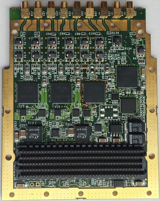
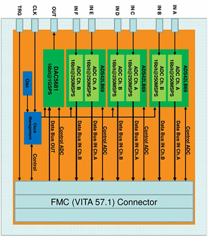
FMC16bit6ADC&1DAC
•3 x Dual ADCs ADS42LB69 by T.I.:
– Resolution: 16 bits;
– Clock up to 250 MHz;
– Instantaneous Bandwidth: 900 MHz;
– Power Dissipation: 1.8 W;
– SNR: 73 dBc@170 MHz (typ)
– SFDR: 87 dBFS@170 MHz (typ).
•DAC DAC5681 by TI:
– Resolution: 16 bits;
– Sample rate up to 1 GSPS;
– Instantaneous Bandwidth: 900 MHz;
– Power Dissipation: 1.0 W @ 1 GSPS, 600 mW @ 500 MSPS, full
operating conditions;
– Single carrier W-CDMA ACLR = 80 dBc @ 80 MHz IF;
– High performance, low noise PLL clock multiplier
– Digital inverse sinc filter.
•Clock Section:
– External Reference up to 350 MHz
– Clock Reference;
– 50 MHz LO (TXCO);
– Distribution of the PLL+VCO output
•Input Trigger signal;
• VITA 57.1 – 2010 compliant (HPC
Connector);
• Conduction Cooled format;
• Conformal Coating (opz);
• Antisulfur resistors (opz);
• Operating Temperature Range: (-40,
+85)°C;
• Operating Humidity Range: 5% to
95% at 40°C non-condensing.
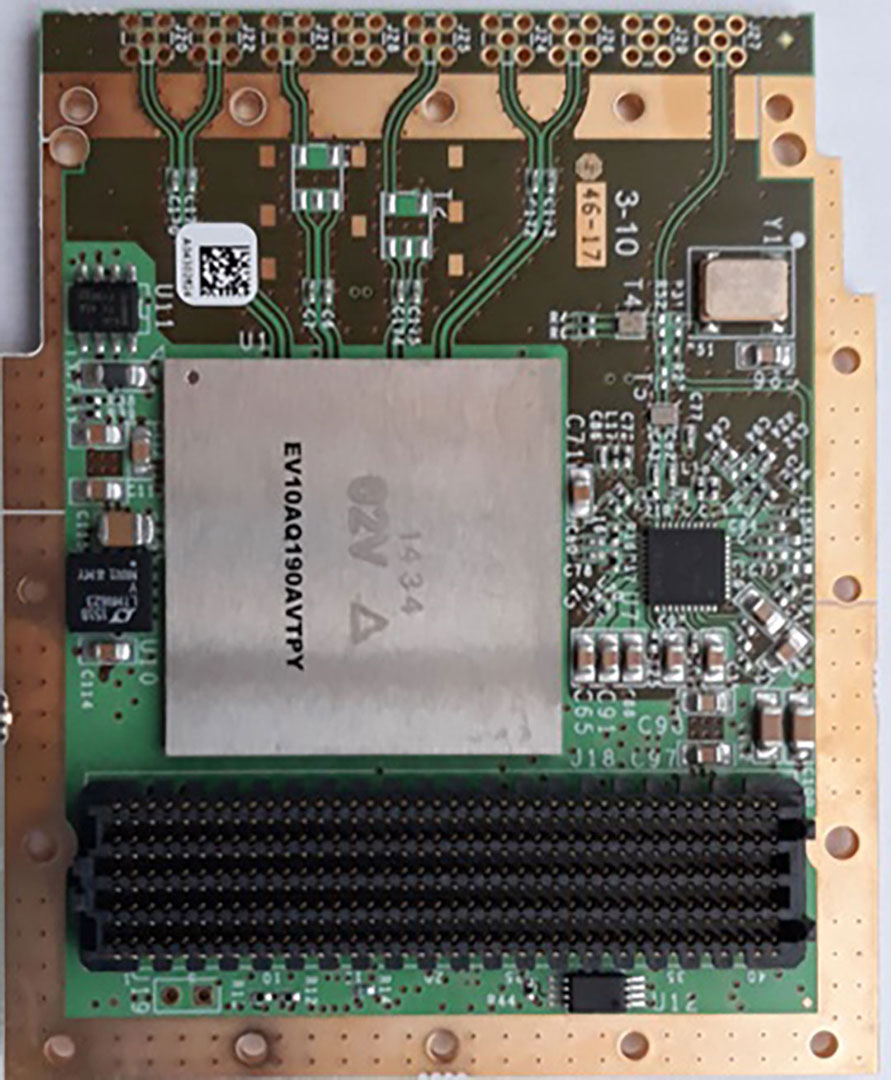
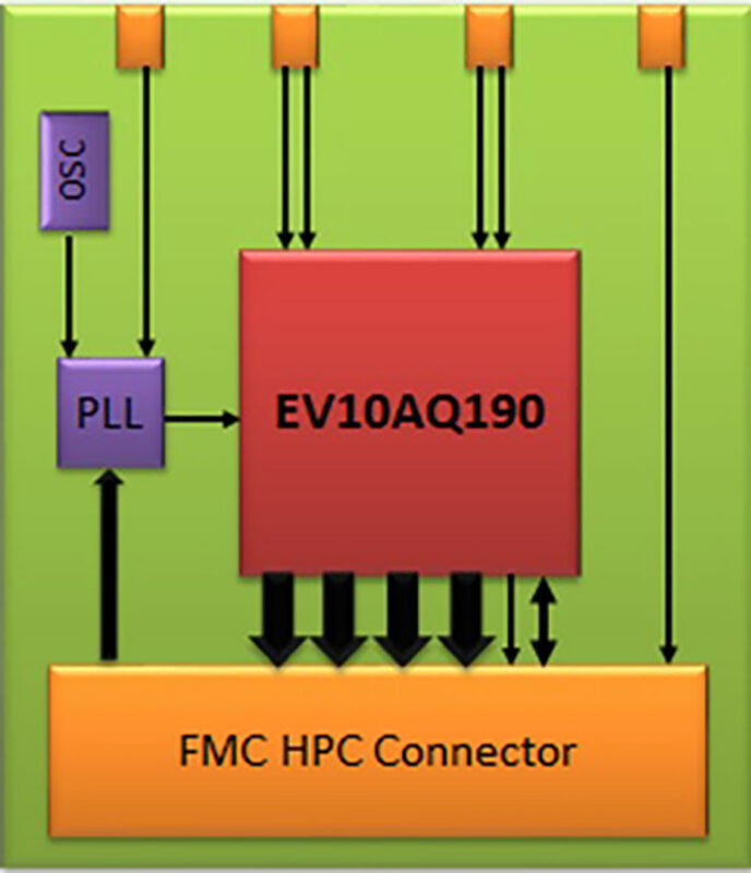
FMC High Speed 10 bit Quad ADC
– Resolution: 10 bits;
– Clock up to 5000 MHz (1-channel conf);
– Four Channels (1, 2 or 4 input configuration):
1. Two Single ended inputs;
2. Two Differiantial inputs (matched).
– Internal clock generation;
– Instantaneous Bandwidth
1. Single ended inputs 40 to 3000 MHz;
2. Two Differiantial inputs up to 3 GHz.
– Power Dissipation: 3 W.
•Internal PLL:
– Internal TCXO;
– External reference (alternative to TCXO);
•External SYNC
•Input SYNC signal;
• VITA 57.1 – 2010 compliant (HPC Connector);
• Conduction Cooled format;
• Conduction Cooled format;
• Conformal Coating (opz);
• Antisulfur resistors (opz);
• Operating Temperature Range: (-40,
+85)°C;
• Operating Humidity Range: 5% to
95% at 40°C non-condensing.
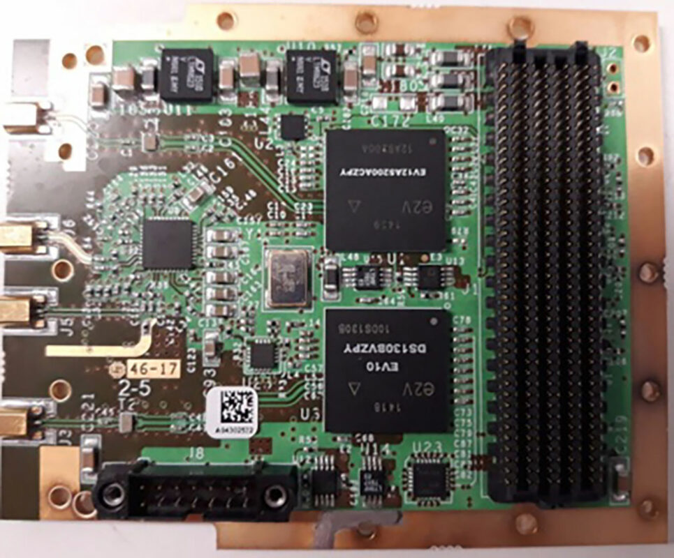
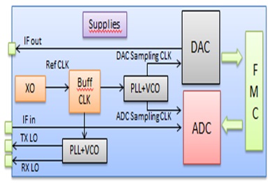
FMC High Speed Dual ADC and DAC
– Resolution: 12 bits;
– Clock up to 1500 MHz;
– Singe ended Input;
– Internal clock generation;
– Instantaneous Bandwidth: 400-3000 MHz;
– Power Dissipation: 3 W.
•DAC EV10DS130 by E2V:
– Resolution: 10 bits;
– Clock up to 3000 MHz;
– Singe ended Output;
– Internal clock generation;
– Instantaneous Bandwidth: 400-3000 MHz;
– Power Dissipation: 1.6 W (MUX 1:2).
•Two internal PLL (Internal TCXO):
– PLL for internal clock generation (ADC, DAC);
– PLL for external clock generation (OUT1, PUT2).
•Input SYNC signal;
• VITA 57.1 – 2010 compliant (HPC Connector);
• Conduction Cooled format;
• Conduction Cooled format;
• Conformal Coating (opz);
• Antisulfur resistors (opz);
• Operating Temperature Range: (-40,
+85)°C;
• Operating Humidity Range: 5% to
95% at 40°C non-condensing.
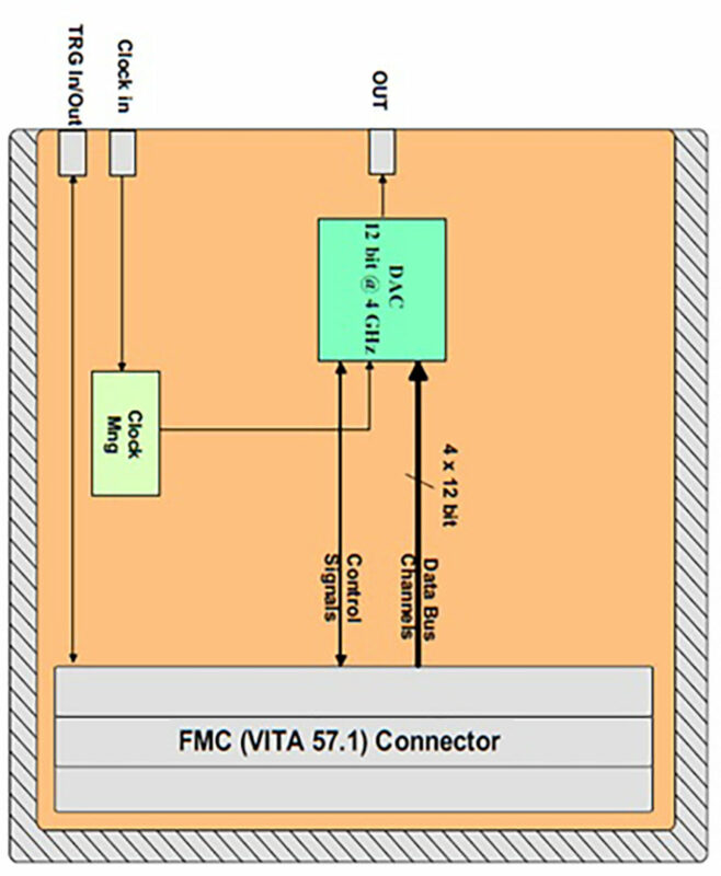
FMC HS SYNTHESIZER
− Single ended (A.C. coupled);
− Up to 3rd Nyquist Band Usable Analog Outputs (Clk = 4 GHz).
•Clk Input Characteristics:
− Single ended clock;
− Direct or PLL Distribution mode;
− PLL Input frequency mode: (0.5 – 350) MHz.
•DAC Characteristics (MD653D by Euvis):
− DAC Resolution 12-bit;
− 1:4 Demultiplexed Digital LVDS Inputs;
− Sampling Clock = 4 GHz;
− True Single Core Architecture;
− Output Voltage Span: 800 mVpp
• 4 W Power Consumption;
• Input Trigger signal;
• FMC format (VITA57.1) Conduction Cooled;
• Operative temperature Range: (-40 , +85)°C;
• Conformal Coating opz.
• FMC IP Cores available (VHDL language)• Input SYNC signal;
• Input SYNC signal;
• Conduction Cooled format;
• Conformal Coating (opz);
• Antisulfur resistors (opz);
•Operating Temperature Range: (-40, +85)°C;
• Operating Humidity Range: 5% to 95% at 40°C non-condensing.
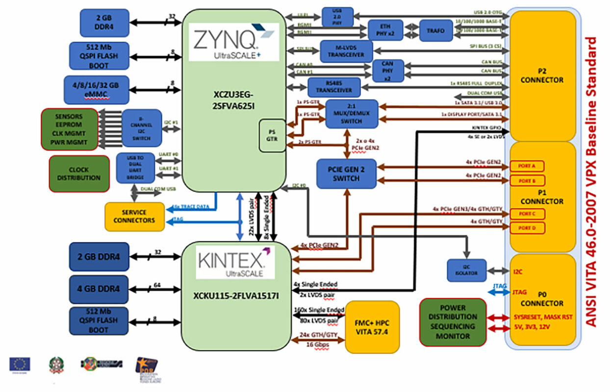
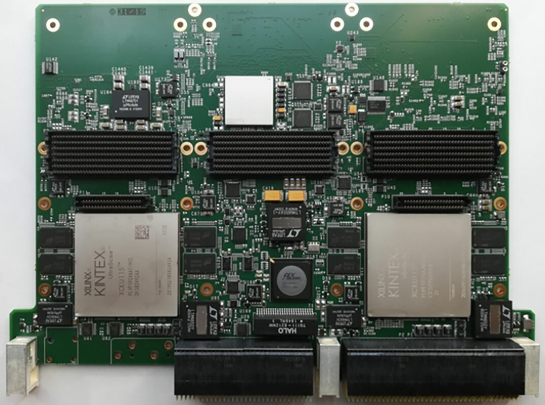
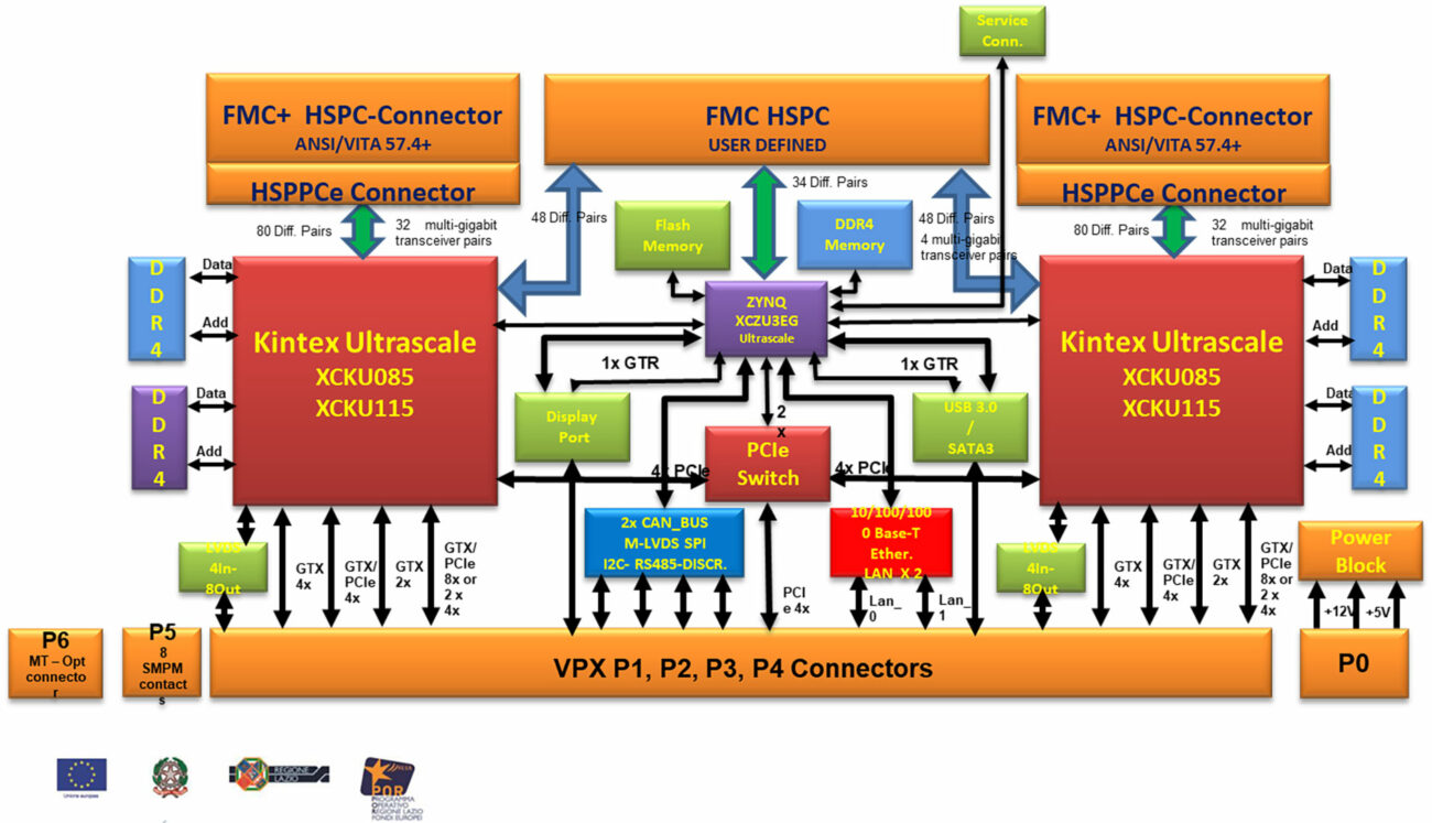
Kintex&ZynqUS_3UVPX_ Board
• ZYNQ: XCZU3EG-2SFVA625I
• ZYNQ external Memory
− DDR4: 2 GB (x32) DDR4 -1600
− Flash Memory : 64 MB
− eMMC: 4/8/16/32 GB
•Processor Peripherals :
− GPIO, 2 x CAN BUS, 2 x I2C, 1 x SPI BUS
• ZYNQ external Memory
− 16 flexible & configurable ports (x1, x4 or x8)
− Four DMA Channels
− Dual Cast
•FPGA: Kintex Ultrascale XCKU115, XCKU095, XCKU085 FLVA1517,
•FPGA external memory:
− DDR4 memory : 1 bank 4 GB (x64) + 1 bank 2 GB (x32) DDR4 -1600
− Flash memory : 64 MB (x8)
− Sampling Clock = 4 GHz;
• Connectors: According to VITA 46.0/VITA 65.0 (P0,P1,P2), and to VITA 57.4 (P3)
• P0 : Power & System signals
• P1 : Two x4 fabric ports mapped as per VITA 46.0, that can be configured as:
− Port A, B : One x4 PCIe Gen2 Port, connected to PCIe Switch
− Port C : One x4 fabric Port (4 lanes connected to FPGA PCIe GEN3 or GTH/GTY)
• P2 : 1x USB 2.0, 2x Gigabit Ethernet, 1x SATA 3.1, 1x DISPLAY PORT, 2x CAN BUS, 1x USB (2x debug UART), 1x SPI
• P3 : FMC high-pin count connector according to VITA 57.4, extended support from 10 to 24 GT + 80 differential pairs
• VPX 3U Air or Conduction cooled Mechanical frame.
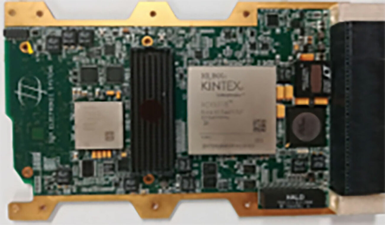
Kintexs&ZynqUS_6UVPX_ Board
• ZYNQ: XCZU3EG-2SFVA625I
• ZYNQ external Memory
− DDR4: 2 GB (x32) DDR4 -1600
− Flash Memory : 64 MB
− eMMC: 4/8/16/32 GB
•Processor Peripherals :
− GPIO, 2 x CAN BUS, 2 x I2C, 1 x SPI BUS
• ZYNQ external Memory
− 16 flexible & configurable ports (x1, x4 or x8)
− Four DMA Channels
− Dual Cast
•FPGA: Kintex Ultrascale XCKU115, XCKU095, XCKU085 FLVA1517,
•FPGA external memory:
− DDR4 memory : 1 bank 4 GB (x64) + 1 bank 2 GB (x32) DDR4 -1600
− Flash memory : 64 MB (x8)
− Sampling Clock = 4 GHz;
• Connectors: According to VITA 46.0/VITA 65.0 (P0,P1,P2), and to VITA 57.4 (P3)
• P0 : Power & System signals
• P1 : Two x4 fabric ports mapped as per VITA 46.0, that can be configured as:
− Port A, B : One x4 PCIe Gen2 Port, connected to PCIe Switch
− Port C : One x4 fabric Port (4 lanes connected to FPGA PCIe GEN3 or GTH/GTY)
• P2 : 1x USB 2.0, 2x Gigabit Ethernet, 1x SATA 3.1, 1x DISPLAY PORT, 2x CAN BUS, 1x USB (2x debug UART), 1x SPI
• P3 : FMC high-pin count connector according to VITA 57.4, extended support from 10 to 24 GT + 80 differential pairs
• VPX 3U Air or Conduction cooled Mechanical frame.
Analog Receiver in Ku band
•Operative bandwidth:(14.1 - 15.7) GHz
•Sensitivity: -150 dBw (-120dBm)
•Maximum input signal: -100 dBw (-70 dBm)
•Noise Figure <9 dB
•Gain chain: 80 dB
•Operative temperature: 25°
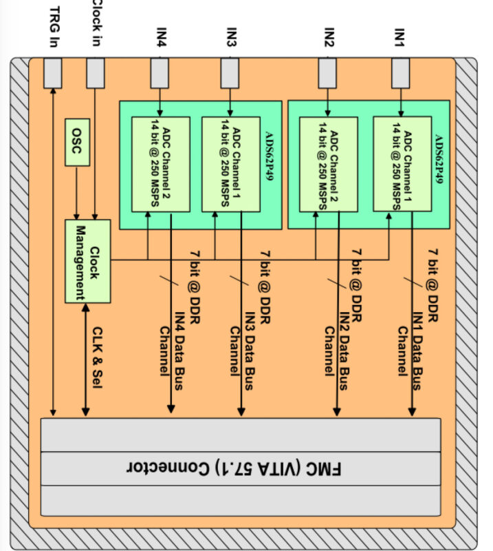
FMC Quad 14 bit ADC
•Two Dual ADCs ADS62P49 by T.I.:
•Resolution: 14 bits;
•Clock up to 250 MHz;
•Input Bandwidth selection (opz.); Instantaneous Bandwidth: 500 MHz; Power Dissipation: 1.25 W; •SFDR: 95 dBc @170 MHz (typ) SINAD: 70 dBFS@170 MHz (typ).
•External or internal Clock Generation;
•Input Trigger signal;
FMC IP Cores available (VHDL language). The front connectors are MMCX type.
•VITA 57.1 – 2010 compliant (HPC Connector);
•Conduction Cooled;
•Conformal Coating (opz);
•Anti-Sulfur Resistor type
•Operating Temperature Range: (-40, +85) °C;
•Operating Humidity Range:
5% to 95% at 40°C non-condensing
Bando KETs
TECNOLOGIE ABILITANTI
Promotore: D. & P. ELECTRONIC SYSTEMS SRL
Impresa Partner: C&C srl
Investimento totale del progetto: 425.204€
Contributo ammesso: 256.413€
Obiettivo:
Realizzazione di VERY HIGH PERFORMANCE PROCESSING UNIT